- 您现在的位置:买卖IC网 > Sheet目录313 > AT45CS1282-TC (Atmel)IC FLASH 128MBIT 50MHZ 40TSOP
Features
? Single 2.7V - 3.6V Supply
? Dual-interface Architecture
– RapidS ? Serial Interface: 50 MHz Maximum Clock Frequency
(SPI Modes 0 and 3 Compatible for Frequencies up to 33 MHz)
– Rapid8 ? 8-bit Interface: 20 MHz Maximum Clock Frequency
?
?
Page Program
– 16,384 Pages (1,056 Bytes/Page) Main Memory
Sector Erase Architecture
– Sixty-three 270,336-byte Sectors
– One 261,888-byte Sector
– One 8,488-byte Sector
128-megabit
?
?
?
?
?
?
?
?
?
Two 1056-byte SRAM Data Buffers – Allows Receiving of Data
while Reprogramming the Flash Array
Continuous Read Capability through Entire Array
– Ideal for Code Shadowing Applications
Low-power Dissipation
– 10 mA Active Read Current Typical – Serial Interface
– 12 mA Active Read Current Typical – 8-bit Interface
– 15 μA CMOS Standby Current Typical
Hardware Data Protection
Security: 128-byte Security Register
– 64-byte User Programmable Space
– Unique 64-byte Device Identifier
JEDEC Standard Manufacturer and Device ID Read
100 Program/Erase Cycles Per Sector Minimum
Data Retention – 10 Years
Commercial Temperature Range
2.7-volt
Dual-interface
Code Shadow
DataFlash ?
AT45CS1282
Preliminary
Description
The AT45CS1282 is a 2.7-volt, dual-interface sequential access Flash memory
ideally suited for infrequent code shadowing applications. This device utilizes Atmel’s
e - STAC ? Multi-Level Cell (MLC) memory technology, which allows a single cell to
?
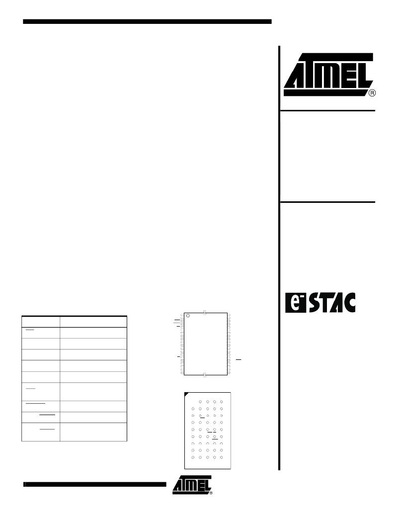
Pin Configurations
TSOP Top View: Type 1
NC
NC
1
2
40
39
NC
NC
Pin Name
CS
SCK/CLK
SI
SO
Function
Chip Select
Serial Clock/Clock
Serial Input
Serial Output
RDY/BUSY
RESET
WP
NC
NC
NC
VCC
GND
NC
NC
NC
NC
CS
SCK
SI*
SO*
NC
NC
3
4
5
6
7
8
9
10
11
12
13
14
15
16
17
18
19
20
38
37
36
35
34
33
32
31
30
29
28
27
26
25
24
23
22
21
NC
NC
NC
I/O7*
I/O6*
I/O5*
I/O4*
VCCP*
GNDP*
I/O3*
I/O2*
I/O1*
I/O0*
SER/BYTE*
CLK
NC
NC
NC
I/O7 - I/O0
8-bit Input/Output
CBGA Top View
WP
Hardware Page Write
Protect Pin
1
2
3
4
5
A
RESET
Chip Reset
B
RDY/BUSY
Ready/Busy
C
NC SER/BYTE NC
I/O7
I/O6
D
SER/BYTE
Serial/8-bit Interface
Control
E
F
I/O2 SCK/CLK GND VCC
I/O1 CS RDY/BUSY WP
I/O5
I/O4
I/O0
SO
SI
RESET I/O3
G
NC
GNDP VCCP
NC
NC
H
Note:
*Optional Use – See pin description text
for connection information.
J
Rev. 3447A–DFLSH–2/04
1
发布紧急采购,3分钟左右您将得到回复。
相关PDF资料
AT45DB011B-XI
IC FLASH 1MBIT 20MHZ 14TSSOP
AT45DB021B-TI
IC FLASH 2MBIT 20MHZ 28TSOP
AT45DB041B-TI
IC FLASH 4MBIT 20MHZ 28TSOP
AT45DB081B-TI
IC FLASH 8MBIT 20MHZ 28TSOP
AT45DB161B-TI
IC FLASH 16MBIT 20MHZ 28TSOP
AT45DB321-TC
IC FLASH 32MBIT 13MHZ 32TSOP
AT45DB321B-TI
IC FLASH 32MBIT 20MHZ 32TSOP
AT45DB321C-TC
IC FLASH 32MBIT 40MHZ 28TSOP
相关代理商/技术参数
AT45CS1282-TI
功能描述:IC FLASH 128MBIT 50MHZ 40TSOP RoHS:否 类别:集成电路 (IC) >> 存储器 系列:- 标准包装:96 系列:- 格式 - 存储器:闪存 存储器类型:FLASH 存储容量:16M(2M x 8,1M x 16) 速度:70ns 接口:并联 电源电压:2.65 V ~ 3.6 V 工作温度:-40°C ~ 85°C 封装/外壳:48-TFSOP(0.724",18.40mm 宽) 供应商设备封装:48-TSOP 包装:托盘
AT45D011
制造商:ATMEL 制造商全称:ATMEL Corporation 功能描述:1-Megabit 5.0-volt Only Serial DataFlash
AT45D011-JC
功能描述:闪存 1M bit
RoHS:否 制造商:ON Semiconductor 数据总线宽度:1 bit 存储类型:Flash 存储容量:2 MB 结构:256 K x 8 定时类型: 接口类型:SPI 访问时间: 电源电压-最大:3.6 V 电源电压-最小:2.3 V 最大工作电流:15 mA 工作温度:- 40 C to + 85 C 安装风格:SMD/SMT 封装 / 箱体: 封装:Reel
AT45D011-JI
功能描述:闪存 1M bit
RoHS:否 制造商:ON Semiconductor 数据总线宽度:1 bit 存储类型:Flash 存储容量:2 MB 结构:256 K x 8 定时类型: 接口类型:SPI 访问时间: 电源电压-最大:3.6 V 电源电压-最小:2.3 V 最大工作电流:15 mA 工作温度:- 40 C to + 85 C 安装风格:SMD/SMT 封装 / 箱体: 封装:Reel
AT45D011-SC
制造商:ATMEL 制造商全称:ATMEL Corporation 功能描述:1-Megabit 5.0-volt Only Serial DataFlash
AT45D011-SI
制造商:ATMEL 制造商全称:ATMEL Corporation 功能描述:1-Megabit 5.0-volt Only Serial DataFlash
AT45D011-XC
制造商:ATMEL 制造商全称:ATMEL Corporation 功能描述:1-Megabit 5.0-volt Only Serial DataFlash
AT45D011-XI
制造商:ATMEL 制造商全称:ATMEL Corporation 功能描述:1-Megabit 5.0-volt Only Serial DataFlash
